-
Call Now
1800-102-2727

Photodiode - Working, Applications, Practice Problems, FAQs

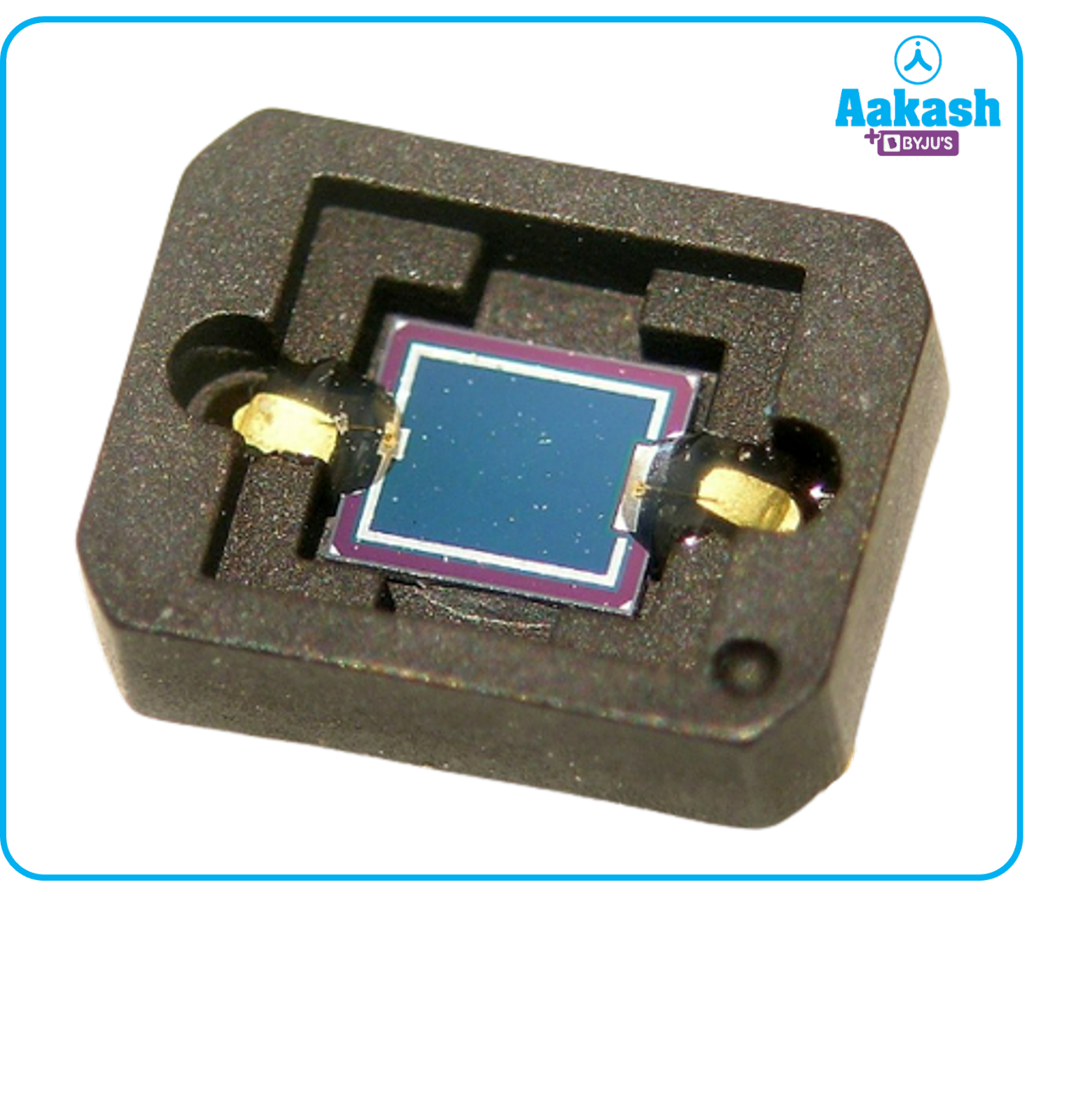
You must have seen the smoke detectors and fire detectors installed in the industrial factories and buildings. Have you ever thought about their working principle? Interesting thing to know is that they are based on the application of photodiodes. They are also utilised in blood gas monitors, computed tomography detectors, and machines that examine samples. Let’s understand the working of photodiodes and its characteristics.
Table of Contents
- Photodiode
- Working of Photodiode
- Applications of Photodiode
- Practice Problems
- FAQs
Photodiode
An electric current is generated by a photodiode, which is a PN-junction diode. Additionally, they go by the names photo-detector, light detector, and photo-sensor. Photodiodes are made to function under conditions of reverse bias. Silicon, Germanium, and Indium Gallium Arsenide are common photodiode materials.
The following image shows the symbol of the photodiode:

When compared to an LED, the photodiode symbol has an arrow pointing inward.
Working of Photodiode
When energy is provided to release electrons from the valence band in semiconductors, current carriers are created. This energy is provided to photodiodes in the form of light energy. A photodiode is a junction diode made of photosensitive semiconductors. The symbol depicted in the figure above serves as its representation. One area of photodiodes is manufactured so narrow that incident light might enter the depletion region.
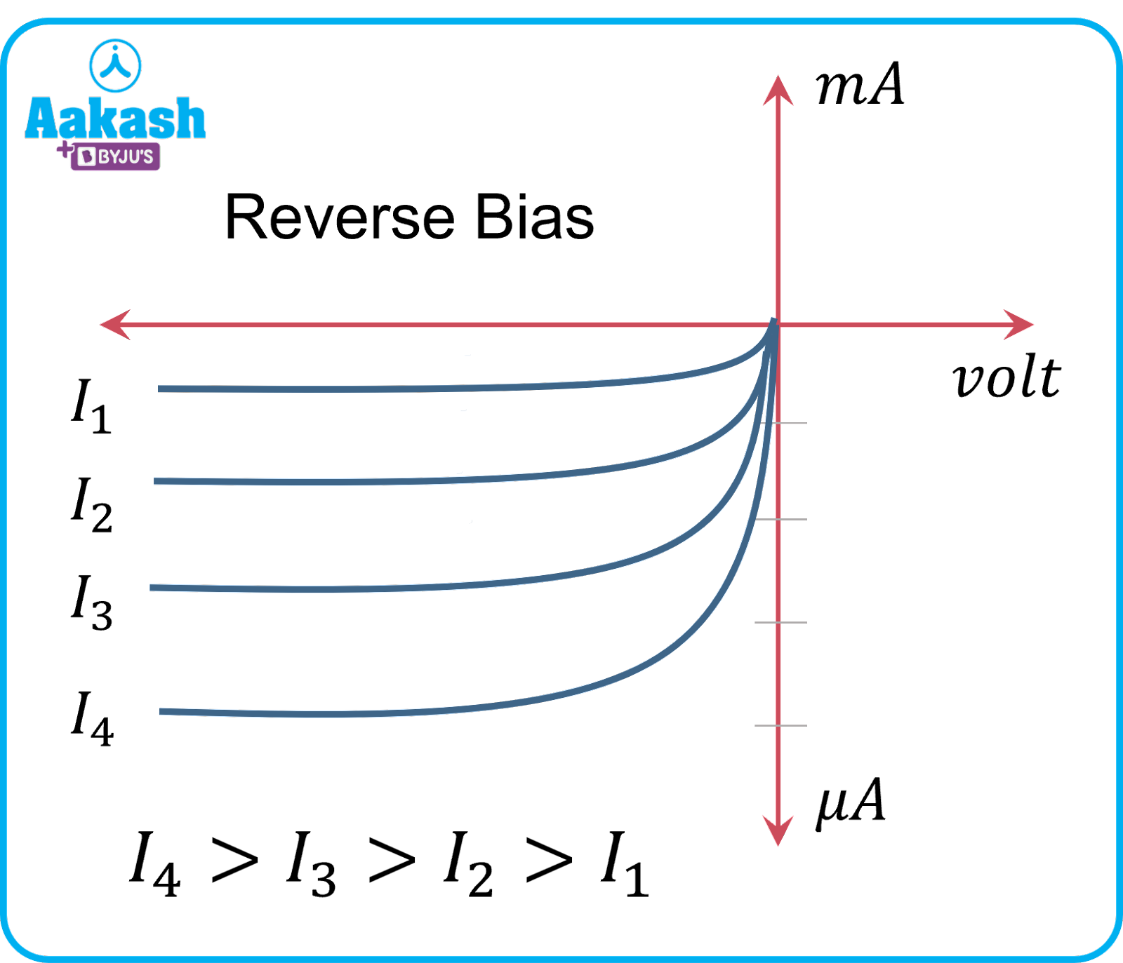
Reverse bias is used to operate photodiodes. Electron-hole pairs are produced when the photodiode is irradiated with energy that exceeds the semiconductor's energy gap (Eg). Electron-hole pairs are produced in or close to the photodiode's depletion zone thanks to the way it is built. The electric field inside the diode causes electrons to accumulate on the N-side and holes to accumulate on the P-side, creating an emf. Therefore, current flows through an external resistance when it is connected. The photocurrent and incident light intensity are inversely related.
A photodiode is connected in reverse bias even though a forward biased photodiode will have a higher photo current because a fractional change in reverse biased current is easier to see when the amount of light shining on it varies. In order to detect optical signals, photo diodes can be utilised as photodetectors. Below is a diagram illustrating typical photo diode I-V characteristics.
Applications of Photodiode
- Simple everyday applications for photodiodes exist. Their widespread use is due to the photodiode's linear response to light irradiation.
- Electric isolation is provided by photodiodes with the aid of optocouplers. Optocouplers are used to optically couple two separated circuits together when they are illuminated by light. When compared to conventional devices, optocouplers are quicker.
- Electronics for safety, such smoke and fire detectors, use photodiodes.
- Numerous medical applications make use of photodiodes. They are also utilised in blood gas monitors, computed tomography detectors, and machines that examine samples.
- Solar cell panels make use of photodiodes.
- Circuits for character recognition use photodiodes.
- In science and industry, photodiodes are used to precisely quantify light intensity.
- For controlling lighting and optical communication, photodiodes are often utilised since they are faster and more complicated than regular PN junction diodes.
Practice Problems
Q. A p-n photodiode is made of a material with a band gap of 4 eV. What is the minimum frequency of radiation that can be absorbed by the material?
A. Given: E=4 eV
E=hf
Q. A photodiode made of semiconductor material having band gap of 2.8 eV. Can it detect on wavelength of 3000 nm?
A. Eg=2.8 eV
λ=3000 nm
As E<Eg , wavelength can not be detected.
Q. The greatest wavelength of photons that a photodiode built of a semiconductor with a bandgap of 3 eV can detect is approximately?
A. Eg=3 eV
Q. A p-n photodiode is made of a material with a band gap of 6 eV. What is the minimum frequency of radiation that can be absorbed by the material?
A. Given: E= eV
E=hf
FAQs
Q. What is the region of operation of a photodiode?
A. Photodiodes operate in reverse biased mode and convert light energy into electrical energy.
Q. When there is no incident light on a photodiode, the reverse current is incredibly small and is known as?
A. When there is no incident light on a photodiode, the reverse current is incredibly small, which is known as dark current.
Q. The recombination of free electrons and holes in a forward-biased diode results in
- Heat
- Light
- Radiation
- All of the above
A. (d) The recombination of free electrons and holes in a forward-biased diode results in heat, light and radiation.
Q. In which region carriers are generated in photodiodes?
- P region
- Depletion region
- N region
- Terminal of the diode
A. (b) In case of photodiodes, carriers are generated in the depletion region.