-
Call Now
1800-102-2727


OR Gate: Truth Table, Symbol, Boolean Expression & Applications

Digital electronics works with signals that exist in two distinct states: LOW (0) and HIGH (1). Unlike the physical world, where quantities change continuously (such as temperature or sound), digital systems operate using clearly defined binary values. These binary states, in fact, allow electronic systems to make decisions based on conditions such as “Yes/No” or “On/Off”.
Now, an OR gate is one of the basic logic gates used in such systems. It produces an output when at least one of the given conditions is satisfied. For example, consider the statement: “I will go to the park if it is sunny OR if my friend comes over.” The action takes place if either one or both conditions are true, which represents the working of an OR gate.
What is an OR Gate?
An OR gate is a fundamental digital logic gate that performs the OR operation (logical addition) on binary inputs. It accepts one or more input signals, each of which can have only two possible states: 0 (LOW) or 1 (HIGH). Then, based on these inputs, it produces a single output, which is also either 0 or 1.
The defining characteristic of an OR gate is its output condition:
- The output becomes HIGH (1) if at least one input is HIGH (1).
- The output is LOW (0) only when all inputs are LOW (0).
This means the OR gate responds to the presence of a HIGH input. Even a single HIGH input is sufficient to make the output HIGH, regardless of the states of the other inputs. In digital circuits, this behaviour is used when an output needs to be activated if any one of multiple conditions is satisfied.
Symbol and Logic Representation
In digital circuits, logic gates are represented using standard symbols that show the relationship between inputs and outputs without displaying internal components.
Now, an OR gate typically has two or more inputs, labelled as A, B, ..., and a single output, usually denoted as Y (sometimes Q or X).

In practical circuits, logic levels are represented using voltages:
- Logic 0 (LOW) corresponds to 0 V (ground)
- Logic 1 (HIGH) corresponds to a positive voltage (typically +5V)
Moreover, the OR gate responds to the presence of a HIGH input. If a HIGH voltage is applied to any one of the inputs, the output becomes HIGH.
This behaviour holds for all cases:
- If A = 1 or B = 1 → output is 1
- If both A and B are 1 → output remains 1
- Only when all inputs are 0 → output is 0
Thus, the output depends on whether at least one input is HIGH, not on all inputs simultaneously.
Truth Table of OR Gate
A truth table serves as a useful diagram that displays all potential input combinations together with their corresponding output results. The standard 2-input OR Gate supports four different input combinations that users can select (22 = 4).
Here is the truth table:
|
|
|
|
|
|
|
|
|
|
|
|
|
|
|
|
|
|
|
|
Explanation of the Table:
- Case 1 (A = 0, B = 0): Both inputs are Low. Since there is no "High" signal coming in from anywhere, the output remains Low (0).
- Case 2 (A = 0, B = 1): Input A is Low, but Input B is High. Because one condition is met, the output goes High (1).
- Case 3 (A = 1, B = 0): Input A is High, and Input B is Low. Again, since at least one input is active, the output goes High (1).
- Case 4 (A = 1, B = 1): Both inputs are High. The OR gate is happy with this; it still gives a High output (1). It does not "cancel out"; it simply stays on.
Boolean Expression of an OR Gate
In digital electronics, the behaviour of logic gates is represented by using Boolean Algebra. This was invented by George Boole.
For an OR Gate, the logical relationship is called Logical Addition. It's written as:
Y = A + B
It is very important to note that the plus sign (+) here does not mean ordinary arithmetic addition.
- In normal maths, 1 + 1 = 2.
- In Boolean logic, 1 + 1 = 1.
Here, the "+" symbol is read as "OR". So, the equation Y = A + B is read as: "Y equals A OR B".
This equation tells us that the output Y will be true (high) if A is true, or if B is true, or if both are true.
Types of OR Gate
OR gates can be classified based on the number of inputs they accept.
You see, as the number of inputs increases, the logic remains the same, but the number of possible input combinations also increases.
1. Two-Input OR Gate
This is the simplest and most commonly used form of an OR gate. It has two inputs (A and B) and one output (Y).
The Boolean expression is written as:
Y = A + B
It produces a HIGH (1) output if at least one of the two inputs is HIGH. Now, for two inputs, the total number of possible input combinations is:

This form is used to understand the basic operation and truth table of the OR gate. The truth table for this type is given as:
|
|
|
|
|
|
|
|
|
|
|
|
|
|
|
|
|
|
|
|
2. Three-Input OR Gate
An OR gate can also have three inputs, usually represented as A, B, and C.
The Boolean expression for this is:
Y = A + B + C
The working principle remains the same:
- If any one of the three inputs is HIGH, the output is HIGH
- The output is LOW only when all inputs are LOW
Now, in the case of three inputs, the total number of combinations is:
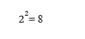
This type is used when more than two conditions need to be checked. The truth table for this type is given as:
|
|
|
|
|
|
|
|
|
|
|
|
|
|
|
|
|
|
|
|
|
|
|
|
|
|
|
|
|
|
|
|
|
|
|
|
|
|
|
|
|
|
|
|
|
3. Multi-Input OR Gate
In general, an OR gate can have “n” number of inputs.
The general Boolean expression is written as:
Y = A + B + C + ...
For an n-input OR gate:

- Output is HIGH if at least one input is HIGH
- Output is LOW only when all inputs are LOW
In practical circuits, multi-input OR gates are often implemented by combining multiple 2-input OR gates.
Realisation of an OR Gate Using Diodes
We can build a simple OR gate using just two P-N junction diodes and a resistor. This helps us understand how the "logic" is actually performed physically.
The Circuit:
- The circuit contains two diodes, which we will name D1 and D2
- The p-side (anode) of D1 connects to Input A.
- The p-side (anode) of D2 connects to Input B.
- Both diodes connect their n-sides (cathodes) to a common point.
- A resistor (R) connects to this common point, which then reaches the ground.
- The system takes Output Y from the resistor connection point, which leads to the diodes connection point.

How it Works (Step-by-Step):
The operation of the circuit depends on whether the diodes are forward-biased or reverse-biased.
- When A=0 and B=0: Both inputs are at 0V. Neither diode is "pushed" to conduct electricity (they are not forward-biased). No current flows through the resistor. Therefore, the voltage at output Y is 0V. (Output = 0).
- When A=1 and B=0: Input A is at +5V. This makes diode D1 forward-biased (it acts like a closed switch). Current flows through D1 and down through the resistor. This current creates a voltage drop across the resistor, making point Y go High (+5V). Diode D2 stays off because its input is 0. (Output = 1).
- When A=0 and B=1: This is the reverse of the previous case. Now, diode D2 is forward-biased by +5V at Input B. Current flows through D2 and the resistor. Point Y becomes High (+5V). (Output = 1).
- When A=1 and B=1: Both diodes are connected to +5V. Both are forward-biased. Current flows through both paths into the resistor. The voltage at Y is still pulled up to the High level (+5V). (Output = 1).
Applications of the OR Gate
- Signal Detection in Electronic Circuits: OR gates are used to detect the presence of a signal from multiple inputs. If any one input becomes HIGH, the output activates, making them useful in sensing and triggering circuits.
- Alarm and Safety Systems: In systems like fire alarms or security circuits, multiple sensors (smoke, heat, motion) are connected through an OR gate. If any one sensor is activated, the alarm is triggered.
- Control Systems: OR gates are used in control circuits where an action should occur if any one of several conditions is satisfied, such as starting a machine from multiple switches.
- Digital Decision-Making Circuits: OR gates are used in logic circuits where multiple conditions independently lead to the same output. This is common in combinational logic design.
- Arithmetic and Logic Units (ALU): OR gates are used inside processors as part of logical operations. They help perform bitwise OR operations in computing systems.
- Data Routing and Selection Circuits: OR gates are used in circuits where signals from multiple sources need to be combined into a single output line.
- Interrupt Systems in Microprocessors: Multiple interrupt signals can be combined using OR logic so that the processor responds if any one interrupt occurs.
Characteristics of the OR Gate
An ideal OR gate responds instantly and operates without loss, but in practical circuits, certain characteristics are considered:
- Output Response: The output becomes HIGH if any input is HIGH. The gate responds to the presence of a HIGH signal at any input.
- Propagation Delay: There is a small time delay between a change in input and the corresponding change in output. In modern circuits, this delay is extremely small, typically in the nanosecond range.
- Power Consumption: Logic gates consume very little power under normal operation. However, power consumption increases when the gate switches states frequently.
- Fan-in: Fan-in refers to the number of inputs a gate can accept. OR gates can have multiple inputs (2, 3, 4, or more), and the logic remains the same: the output is HIGH if any input is HIGH.
In the end, an OR gate is a fundamental building block in digital electronics, used wherever an output must be produced based on the satisfaction of any one condition. Its simple logic and wide applicability make it essential for understanding and designing digital circuits.

 Call Now
 Let's Chat
 Share
Share