-
Call Now
1800-102-2727

Intrinsic Semiconductor, Practice Problems, FAQs

In today’s world our life is surrounded by so many electronic devices such as smartphones, laptops, televisions etc. What is the core material that is used for the functioning of these devices? It is none other than the semiconductor material. The properties of semiconductors are very unique. So they have high demand in the industry. The semiconductors which do not have any impurities means they are pure, are called intrinsic semiconductors. In this article we will be studying the properties of pure semiconductors.
Table of Contents
- Intrinsic Semiconductor
- Energy Band
- Conduction Process
- Conductivity
- Practice Problems
- FAQs
Intrinsic Semiconductor
Chemically pure semiconductors are those that lack impurities or are intrinsically pure. The amount of holes and electrons is therefore controlled by the properties of the material rather than by impurities. The ratio of excited electrons to holes is n = p in intrinsic semiconductors. They are also known as semiconductors that are undoped or i-types. Silicon and germanium are examples of materials used in i-type semiconductors. Both of these elements are in the IV th group of the periodic table and have atomic numbers of 14 and 32, respectively.
So in intrinsic semiconductors, Number of Electrons per unit volume = Number of holes per unit volume
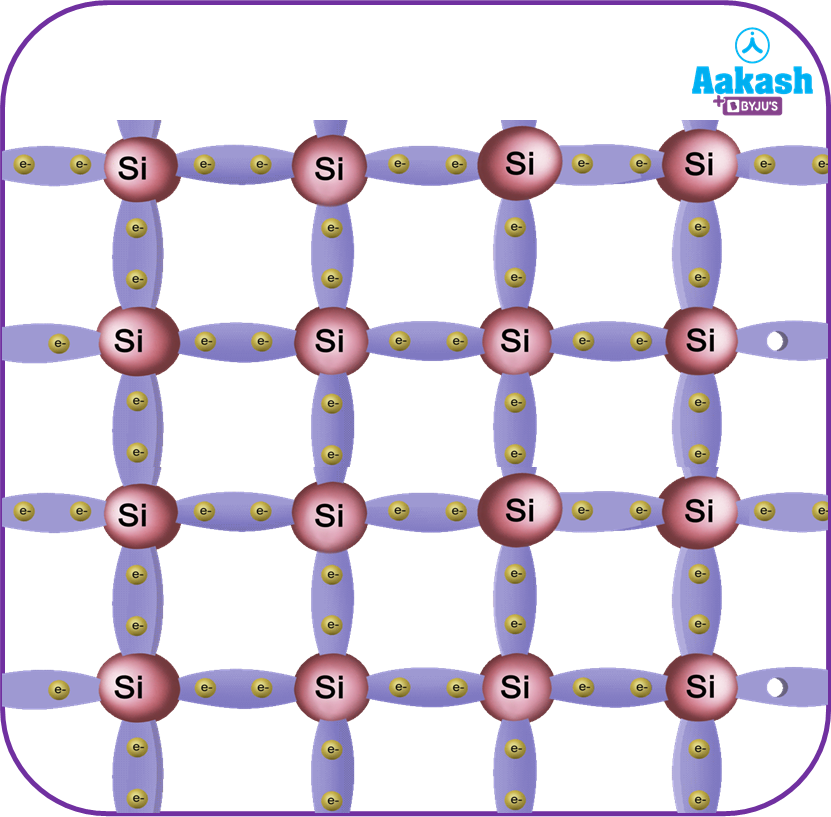
The most frequent types of semiconductors are Ge and Si, whose lattice structures are described as having a diamond-like structure. Each atom in this configuration is surrounded by its four closest neighbours. There are four valence electrons in Si and Ge. Every Si or Ge atom tends to share one of its four valence electrons with each of its four nearest neighbours in its crystalline structure. Thus, covalent bonds are created by the shared electrons (also called valence bonds). The two shared electrons between the connected atoms move back and forth, firmly keeping them together. The two-dimensional schematic representation of the Si and Ge structure is shown in figure.
This is a perfect image where there are no bonds broken and all bonds are present. Low temperatures give rise to this circumstance.
Conduction Process
A portion of these bound electrons gain thermal energy and become free as the temperature of these semiconductors rises. Semiconductors' ability to conduct electricity is aided by these free electrons and empty bonds. The vacancy in the bond is shown in the figure below because only a small fraction of the atoms in the crystalline lattice can be ionised by thermal energy.
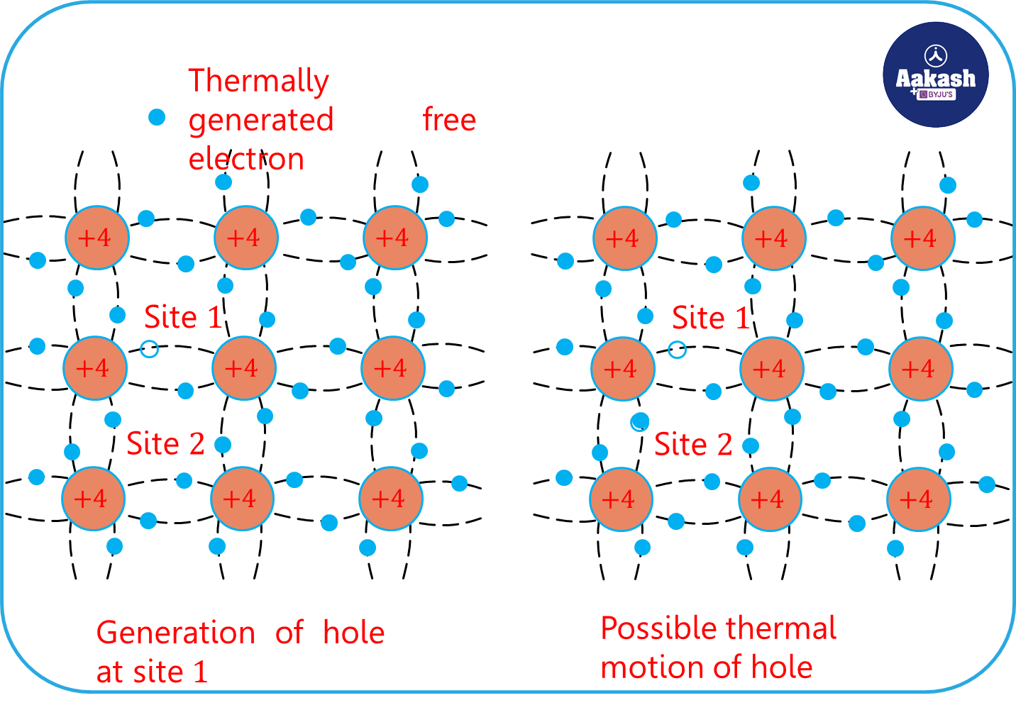
A gap or vacancy with an effective charge (+q) results from the environment where the free electron with charge (-q) has emerged. This empty space with an apparent positive electric charge is referred to as a "hole." The hole behaves as if it were a free particle with a real positive charge.
In intrinsic semiconductors, the number of free electrons per unit volume (n) is equal to the number of holes per unit volume (p) and it is also equal to the number of intrinsic charge carriers per unit volume(ni). Here (ni) is known as intrinsic carrier concentration. Mathematically, we have the relation n = p = ni for intrinsic semiconductors. Due to a special feature of semiconductors, holes in addition to electrons can conduct electricity. Assume site 1 has a hole, as indicated by the first figure. The second picture depicts the movement of holes. It is possible for an electron from the covalent bond at site 2 to move to the open site 1 (hole). A result of this jump is that site 1 now has an electron and site 2 has a hole. This is equivalent to the hole moving from site 1 to site 2. In other words, It is crucial to keep in mind that the hole's motion is unrelated to the electrons that were initially set free in the first figure. Rather the free electron moves independently as a conduction electron which produces electron current (Ie) when some external electric field is applied. Also remember that the motion of hole is only a convenient way of describing the actual motion of bound electrons. Under the action of an electric field, these holes move towards negative potential and this creates the hole current (Ih). Hence, the total current (I) is the sum of electron current and hole current.
I = Ih + Ie
Energy Band
An intrinsic semiconductor behaves like an insulator at absolute zero temperature (i.e. at 0 K) shown in figure.
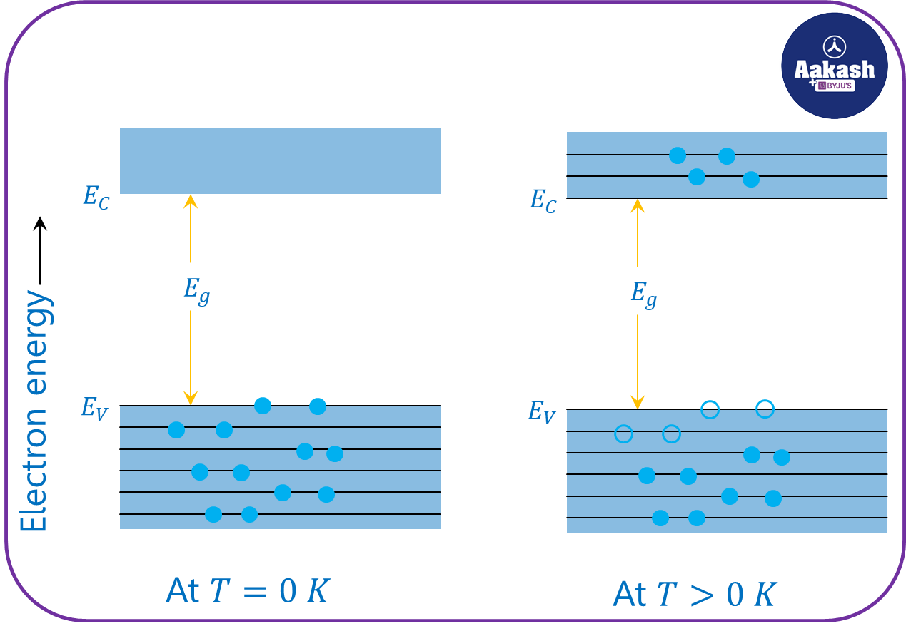
At temperature higher than zero kelvin the thermal energy excites some electrons which are from the valence band to the conduction band. Those thermally excited electrons at temperature, T > 0 K, partly occupy the conduction band. The energy band diagram of an intrinsic semiconductor is shown in figure. Note that, here some electrons have been shown in the conduction band which have come from the valence band creating an equal number of holes in the valence band itself.
Mass Action Law
In a semiconductor, at thermal equilibrium the product of electron concentration and hole concentration is equal to the square of the intrinsic concentration.
np = ni2
Conductivity
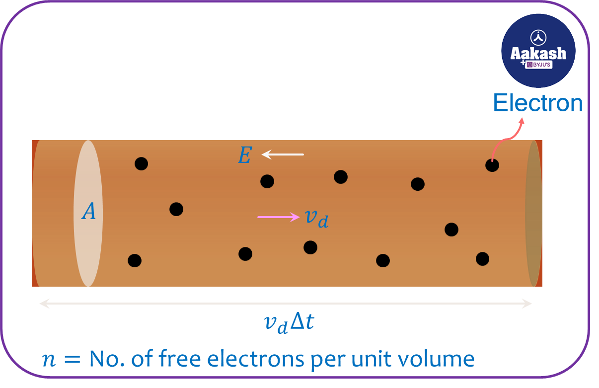
The rate of charge flow with relation to time is known as current. Let vd be the drift speed and n is the number of charge carriers per unit volume, e is charge on electrons, A is the area of cross section. In one second, the distance covered by charge carriers is vd . So the volume covered in one second is Avd. Total number of carriers in one second is nAvd. So total charge transferred in one second is neAvd. So we can write
I = neAvd……(1)
There is relation between mobility of charge carriers μ and drift speed vd and the electric field E.


Now, 


 ………(2)
Here, J=Current density
From Ohm’s Law,
 …………(3)
Here,
E = Electric field
By comparing equation (2) with (3)

In case of a semiconductor, conductivity is because of the two carriers i.e. electrons and holes. So, 
Here,


For intrinsic semiconductor 

Video Explanation:
Practice Problems
Q1. From the following 14th group elements which one is not a semiconductor?
- C
- Ge
- Si
- All are semiconductor
A. (a) Carbon is not a semiconductor. So option (a) is correct.
Q2. Find the intrinsic concentration of the semiconductor having electron concentration of n = 5 X 1018 cm-3.
A. For intrinsic semiconductor, electron and hole concentration is equal and both are equal to the intrinsic concentration.
So n = p = ni = 5 x 1018 cm-3
Q3. Find the mobility of electrons having drift speed of 4102 ms-1 after the application of 2000 Volt m-1 electric field.
A. vd = 4 x 10² ms-1
E=2000 Volt m-1


Q4. Find the conductivity of intrinsic semiconductor having carrier concentration of  . Electron and hole mobility is
  and
and  respectively.
A. 


FAQs
Q1. At what temperature does the intrinsic semiconductor behave as an insulator?
A. At absolute zero temperature intrinsic semiconductor acts as insulator as there are no free charge carriers for the conduction of current.
Q2. Consider Ih and Ie be the current due hole concentration and electron concentration then the total current (I) through the semiconductor,
- I = Ih - Ie
- I = Ie - Ih
- I =Ih+Ie
- N one of the above
A. Electron and hole concentration both contribute to the flow of current in the same direction. So, net current through the semiconductor is I = Ih + Ie.
Q3. At room temperature the concentration of electrons and holes in intrinsic semiconductor is,
- Equal
- Zero
- Electron concentration is greater than hole concentration
- Hole concentration is greater than electron concentration
A. In the case of an intrinsic semiconductor, hole and electron concentration are the same. So option (a) is correct.
Q4. At 0 K, what type of behaviour is shown by Germanium?
- Conductor
- Semiconductor
- Insulator
- None of the above
A. (c)
At absolute zero temperature there are no carriers in the conduction band for a semiconductor. Germanium, being a semiconductor, acts as an insulator at 0 K.