-
Call Now
1800-102-2727


Zener Diode - Working, V-I characteristics, Practice Problems, FAQs
Electronic devices require constant voltage supply for their operation. Consider your laptop requires a specific amount of voltage to function properly which is generally around 19 V. If for some reason the supply voltage is increased, it might damage certain components that are present inside the laptop and it will stop functioning properly. Here comes the important application of the zener diode which is widely used as a voltage regulator.
Table of Contents
- Zener diode
- Working of zener diode
- V-I characteristics of zener diode
- Specifications of zener diode
- Practice problems
- FAQs
Zener diode
A zener diode is a specifically engineered, highly doped p-n junction with an extremely thin depletion layer and a sharp breakdown voltage. It is always performed at the breakdown region. Its breakdown voltage VZ is below 6 V.
The first person to describe the electronic properties of a Zener diode was Clarence Melvin Zener. Theoretical physicist Clarence Zener was employed by Bell Labs. His contributions led to the Zener diode being named in his honour.
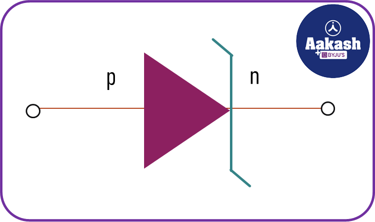
At high reverse breakdown voltages, the reverse current in conventional junction diodes increases quickly. With reverse breakdown voltage, junction diodes with low power ratings are destroyed. Zener diodes are junction diodes that have been carefully developed to operate constantly in the reverse breakdown voltage range without being damaged. These silicon diodes are often heavily doped. Due to its greater thermal stability, silicon is preferable to germanium. Below is a symbol that is used to represent a zener diode.
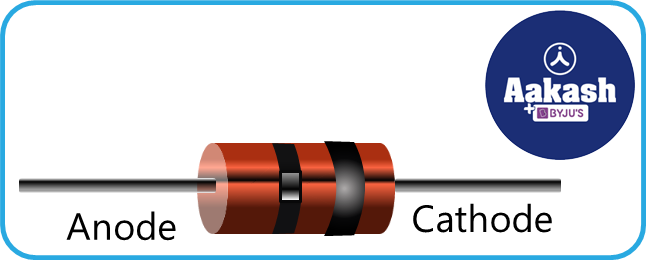
Following image shows the actual zener diode that is used in electronic circuits.
Working of zener diode
When it is forward biased, a Zener diode behaves just like a regular diode. However, when coupled in reverse biased mode, a tiny leakage current passes through the diode. Current begins to flow through the diode as the reverse voltage rises to the predetermined breakdown voltage (VZ). The series resistor-determined maximum current is reached before the current stabilises and remains constant throughout a broad range of applied voltage. There are two types of breakdown diodes i.e. Avalanche Breakdown and Zener Breakdown. In the case of a zener diode, Zener Breakdown occurs.
- Avalanche Breakdown
This kind of breakdown occurs in a reverse bias of a lightly doped p-n junction. When the p-n junction is lightly doped, the width of the depletion region is large. Hence, when reverse bias is applied, some covalent bonds are broken in the depletion region and electron holes are produced in pairs. These freed electrons move towards the n side under the influence of a barrier electric field, which again collides with atoms producing further electron hole pairs. This results in a continuous flow of current carriers in reverse bias and these newly generated charge carriers are also accelerated by an applied electric field in reverse bias leading to avalanche breakdown.
- Zener Breakdown
This breakdown occurs in a highly doped p-n junction in which the width of the depletion region is small. When reverse bias voltage is increased, the electric field across the depletion region also increases (which is the sum of barrier electric field and applied electric field) and if we go on increasing the reverse bias voltage, at a particular value (called Zener voltage) a large number of electrons and holes are produced. This is called Zener breakdown.
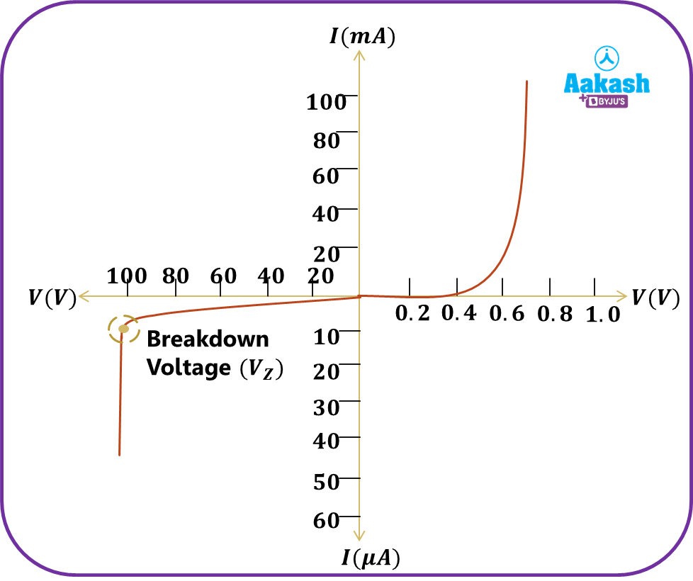
V-I characteristics of zener diode
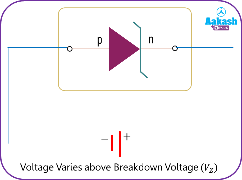
In the following circuit we have applied reverse bias voltage to zener diode and plotted I vs V curve to understand the characteristic of the zener diode.
The forward characteristics of a Zener diode are shown in the graph's first quadrant. We can infer from the graph that its forward characteristics are essentially the same as those of any other P-N junction diode.
Initially, in reverse bias, the current is almost constant with an increase in magnitude of voltage. But, at breakdown voltage, the electric field is so high that it takes away the electrons from its core. This increases the number of charge carriers to such an extent that the current increases drastically. This is called Zener breakdown. Even though the current is changing, the voltage is constant. Therefore, the Zener diode is reverse biased and is used as a voltage regulator to get constant voltage output. In normal diodes a similar phenomenon takes place, but there the mechanism is avalanche breakdown in which free electrons knock off bonded electrons.
Specifications of zener diode
Here are some specifications of a zener diode that are considered before using it in any electronic circuit.
- Zener Voltage (VZ): It is the reverse bias breakdown voltage at which the P-N junction goes into zener breakdown. Generally it ranges from 2.4 V to 200 V.
- (IZ)min: It is the minimum reverse bias current when the zener diode undergoes reverse bias breakdown. It is also known as Knee Current.
- (IZ)max: It is the maximum current that a zener diode carries in reverse bias at a given rated zener voltage.
- Power Rating: It is the maximum power that a zener diode can dissipate without getting damaged. It can be calculated using,
- Zener Resistance (RZ): It is the opposition offered by the zener diode to the flow of current flowing through it in the operating region.
Practice problems
Q. Find the power rating of zener diode having breakdown voltage of 12 V and reverse bias current varies from 20 mA to 2 A.
A. Zener voltage, VZ=12 V
the power rating of the zener diode can be found as,
Q. V-I characteristics of zener diodes are shown in the figure below. Find the knee current and power rating of the diode.

A. From the figure
VZ=100 V
So the power rating of the zener diode,
Q. Avalanche breakdown is due to,
- collision of minority charge carrier
- increase in depletion layer thickness
- decrease in depletion layer thickness
- none of these
A. In reverse bias, at breakdown voltage the electric field is so high that minority electrons gain so much velocity and hence, they knock off the bonded electrons. Due to this the concentration of charge carriers increases and hence the current increases drastically. Therefore, avalanche breakdown is due to collision of minority charge carriers. Thus, option (a) is the correct answer.
Q. On increasing the reverse bias to a large value in a pn-junction diode, current (pick the right one)
- increases slowly
- decreases slowly
- remains fixed
- suddenly increases
A. In reverse bias, the current is almost constant initially. But, at breakdown voltage there is a tremendous increase in the current because of the zener breakdown or avalanche effect. So option (d) is correct.
FAQs
Q. How is a zener diode different from a normal semiconductor diode?
A. The direction of flow of current is where a Zener diode and a normal diode differ the most. The normal circuit diode is used to block the current flow in reverse condition and generally it is operated in forward bias and with high reverse bias voltage it may get damaged. The zener diode works the same as normal diodes during forward bias. But generally it is operated in a reverse bias condition. As it has a high breakdown voltage it can sustain large values of currents and voltage in reverse bias, which is used in voltage regulators.
Q. Does a zener diode work in forward bias?
A. Yes, zener diodes work in forward bias in the same way as the other junction diodes. The current is low in forward bias. They are mainly operated in the reverse breakdown region.
Q. What is the use of a zener diode?
A. Zener diodes can be used as over-voltage protection in the reverse breakdown region. In reverse breakdown condition it has constant voltage output. So if there is a high voltage supply which could damage the device, with the help of a zener diode we can protect the circuit. It can also be used in clipping circuits.
Q. What is the main difference between avalanche breakdown and zener breakdown?
A. Avalanche breakdown occurs in a reverse bias of a lightly doped p-n junction. When the p-n junction is lightly doped, the width of the depletion region is large. Hence, when reverse bias is applied, some covalent bonds are broken in the depletion region and electron holes are produced in pairs. Zener breakdown occurs in a highly doped p-n junction in which the width of the depletion region is small. When reverse bias voltage is increased, the electric field across the depletion region also increases (which is the sum of barrier electric field and applied electric field) and if we go on increasing the reverse bias voltage, at a particular value (called Zener voltage) a large number of electrons and holes are produced. With a breakdown voltage of up to 5.6 volts, the avalanche effect predominates; above that, the zener effect becomes dominant.