-
Call Now
1800-102-2727

Forward Bias Diode- Depletion Width, Practice Problems, FAQs

We see a one-way sign board on the roadside. That means vehicles are allowed to travel in only one direction. If we want to implement a similar phenomenon in the case of an electronic circuit where current will be allowed to pass in only one direction then we can make use of a p-n junction diode. A p-n junction is formed by the combination of p-type and n-type semiconductors. It has a variety of applications such as solar cells, LED etc. In this article we will be studying about the forward biassing of the diodes in detail.
Table of content:
- p-n Junction Biassing
- Forward Bias
- V-I Characteristics of p-n junction
- Advantages of p-n Junction
- Practice Problems
- FAQs
p-n Junction Biassing
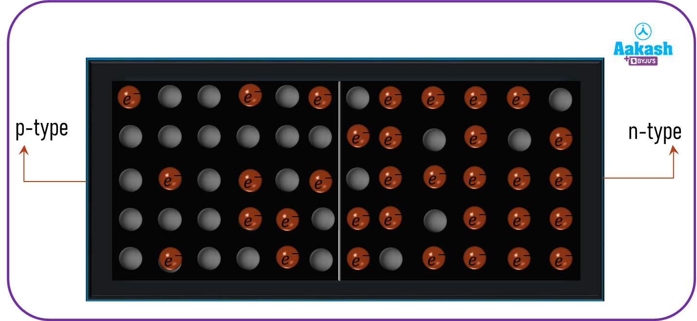
A pure semiconductor develops electrons and holes, two different types of charge carriers and significantly increases its conductivity when impurities are added to it. Many p- and n-type semiconductor devices have been developed using this fact. p and n type semiconductors alone have restricted applications. The p-n unit, also known as the p-n junction diode, is created when the two types are joined together. This combination has a variety of novel properties that make it a particularly valuable device. When a p-type semiconductor is grown into an n-type semiconductor or an n-type semiconductor is grown into a p-type semiconductor, a p-n junction is created.
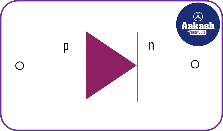
In an electronic circuit the p-n junction is represented by the following symbol.
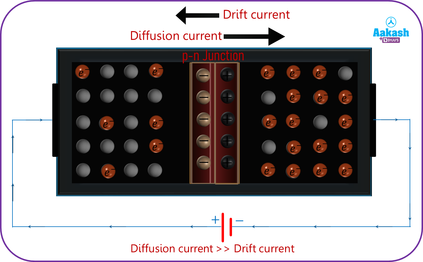
A p-n junction's n-region has a larger concentration of free electrons than its p-region which has a far higher concentration of holes than free electrons. Therefore, some electrons from the n-region (where their concentration is large) will drift into the p-region when a p-n junction forms (where their concentration is low). Since the hole is nothing more than an electron's vacancy, the covalent bond is completed when an electron diffuses from the n- to the p-region. The name of this procedure is electron-hole recombination.
The electrons in the n-region (close to the junction) are neutralised by holes as a result of the electron-hole recombination, leaving only ionised donor atoms (positive charges) in this small region, as indicated in the figure. In a tiny area close to the junction, the positive and negative ions are bonded and immovable. The depletion region is that tiny area close to the junction that is depleted of free charge carriers (holes and electrons) and contains solely stationary ions.

As a result of the accumulation of positive and negative immobile charges in the depletion region, an electric field (EB) is established in this region. The direction of the field is from the n-region to the p-region, as shown in figure. It is clear that the field will oppose any further flow of electrons from the n-region to the p-region and that of holes from the p-region to n-region. Thus, the electric field causes a potential barrier VB at the junction which prevents further diffusion of electrons and holes into the opposite sections of the depletion regions. This happens because the overall negative charge of the p-region becomes sufficient to repel the free electrons in the n-region, preventing them from crossing the junction and similar is the case with holes in the n-region. This limits the size of the depletion region.
Due to the existence of the potential barrier VB across the junction, an electron from the n-region can cross the junction only if its energy greater than eVB be supplied to it from outside. An equal amount of energy is required to move a hole from the p-region to cross over to the n-region across the barrier. The value of the potential barrier for germanium is about 0.3 V and for silicon about 0.7 V. The size of the depletion region is a few microns.
Forward Bias
We have seen that the majority carriers, which are free electrons in the n-section and holes in the p-section, have a natural inclination to unite at the junction. The important thing to remember is that electrons can travel in the same direction in both p and n-sections because of the way that electrons and holes combine at the junction.
The recombination of electrons and holes is prevented by the potential barrier that develops in a p-n diode alone. If a battery is connected to the diode to overcome this potential barrier, the current flow can resume. If the external battery's polarity is such that the majority carriers in both sections are compelled toward the junction, this type of biassing—known as forward bias—causes the majority carriers to produce the current flow.
It is possible to obtain forward bias by connecting the battery's negative terminal to the n-region and its positive terminal to the p-region. This is because the negative terminal will push free electrons in the n-region away from the junction and the positive terminal will push holes toward the junction, where they will combine. The valence electron from the p-region will leave for the battery for every combination, while a free electron from the battery will enter the n-region. The effect is that the current will flow.
V-I Characteristics of p-n junction
The V-I characteristic of a junction diode is shown in the following figure. With increasing forward bias the current first increases linearly up to a certain forward biassed voltage called cut-in voltage and beyond which the current varies non-linearly.
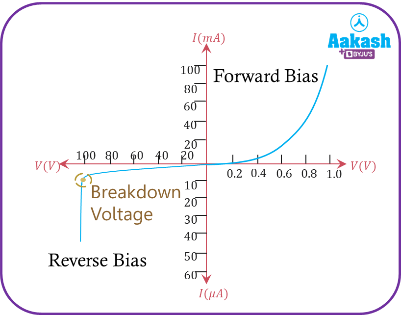
When there is a reverse bias, the reverse current, also known as the reverse saturation current, is unaffected by the reverse bias voltage and only depends on the junction's temperature. The reverse saturation current (Io) is observed to increase by roughly 7% for every 10C rise in temperature. In other words, the Io roughly doubles for every 10°C increase. If we keep raising the reverse bias voltage, the reverse current will suddenly grow for a certain value. This is called the Breakdown voltage.
Advantages of p-n Junction
- The p-n junction diodes do not produce a humming noise during the operation.
- The p-n junction diodes are set into operation as soon as the circuit is switched on.
- The p-n junction diodes require low voltage for their operation. Hence there is low power consumption.
- They are very compact.
Practice Problems
Q1. From the following 14th group elements which one is not a semiconductor?
- C
- Ge
- Si
- All are semiconductor
A. (a) Carbon is not the semiconductor. So option (a) is correct.
Q2. Let VA and VB denotes the potentials of A and B, then the equivalent resistance between point A and B in the following circuit,

- 10 Ohm if VA > VB
- 5 Ohm if VA > VB
- 10 Ohm if VA < VB
- 5 Ohm if VA < VB
A. If VA > VB,
In this case the diode will be forward biassed and behave as a short circuit. So both resistance will be in parallel. So equivalent resistance between A and B will be
If VA < VB,
In this case the diode will be in reverse bias and will act as an open circuit. So equivalent resistance between A and B will be,
R=10 Ohm
So option (b) and (c) are correct.
Q3. In the diagram shown below find the value of current flowing through 300 Ohm resistance?

a. 10 mA
b. 1 mA
c. 0.1 mA
d. 0 mA
A. In the given circuit, anode is at lower potential as compared to cathode. So the diode is in reverse bias. It will not carry any current through the resistor. So the answer is (d) 0 mA.
Q4. Which of the following diodes is forward biassed?
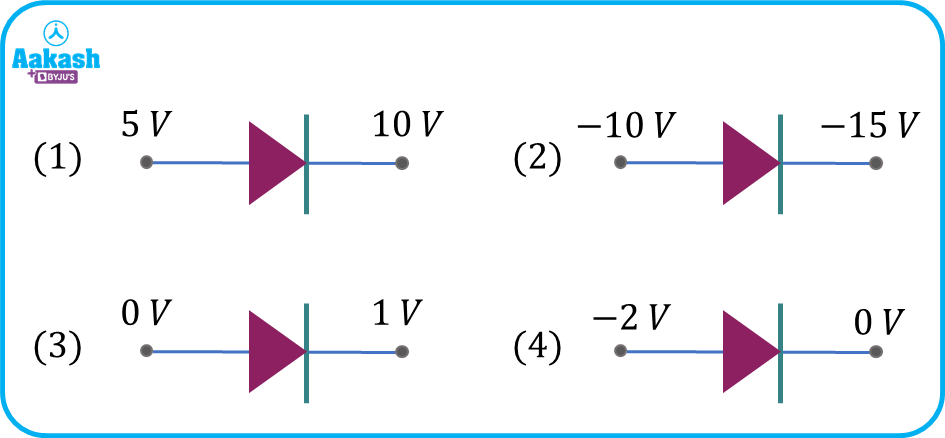
A. For the diodes (1), (3), (4) anode voltage is less than cathode voltage (VA < VC) so they are in reverse bias. But for diodes (2) VA = -10 V and VC = -15 V. Therefore VA > VC That means the diode is forward biassed. So option (2) is correct.
FAQs
Q1. What is meant by an ideal diode?
A. The diode which has zero voltage drop and zero forward bias resistance, also acts as an open circuit in reverse bias, is known as an ideal diode.
Q2. Can we apply Ohm’s law to semiconductor diodes?
A. Semiconductor does not obey Ohm’s law so we can not apply Ohm’s law to it.
Q3. What is the effect of forward bias on the width of the depletion region?
A. Under forward bias conditions the width of the depletion region decreases. In the forward biassed state the applied voltage pushes both the holes (in the p type region) and the electrons (in the n type region) towards the depletion region, thus decreasing its width.
Q4. Consider Ih and Ie be the current due to hole concentration and electron concentration respectively. Then the total current (I) through the semiconductor in forward bias will be,
- I = Ih - Ie
- I = Ie - Ih
- I = Ih + Ie
- None of the above
A. Electron and hole concentration both contribute to the flow of current in the same direction. So net current through the semiconductor is I = Ih + Ie.