
In the realm of electrical engineering and semiconductor physics, certain phenomena hold the key to both innovation and potential risks. One such phenomenon is avalanche breakdown, a fascinating process that occurs within diodes and other semiconductor devices. Let’s embark on a journey to understand what avalanche breakdown is, how it occurs, and its significance in various applications.
The Basics: Diodes and Semiconductor Devices
Before delving into avalanche breakdown, let’s briefly review the foundation: diodes and semiconductor materials. Diodes are fundamental components in electronics that allow current to flow in one direction while blocking it in the opposite direction. They are constructed using semiconductor materials, which have a unique property – they can act as insulators under certain conditions and conductors under others.
Semiconductor materials, like silicon and germanium, are made up of atoms with four valence electrons. This property makes them suitable for forming covalent bonds with neighboring atoms, creating a lattice-like structure. However, this crystal structure also leaves “holes,” or spaces where an electron should be but isn’t. These holes can move within the lattice, allowing for electron movement and conductivity.
The Avalanche Effect: What is Avalanche Breakdown?
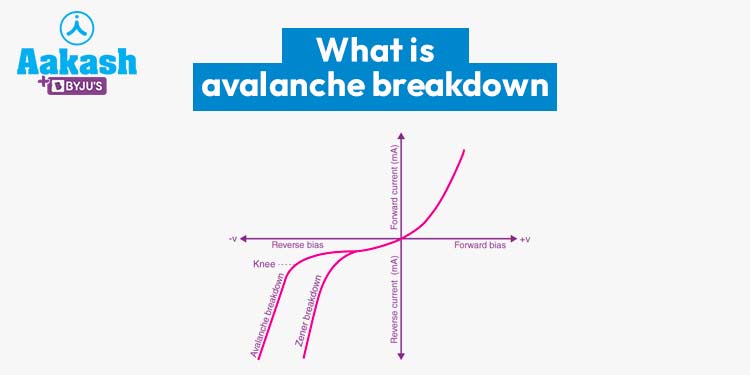
Avalanche breakdown occurs in semiconductor diodes when a reverse bias voltage is applied across them. In simpler terms, this means that the voltage is applied in the direction opposite to the diode’s normal operating mode. When the reverse bias voltage surpasses a certain threshold, an interesting phenomenon unfolds.
At this critical voltage, high-energy free electrons gain enough momentum from the applied electric field to collide with other electrons. These collisions free additional electrons from their covalent bonds, creating even more free electrons and holes. This creates a chain reaction, often described as an “avalanche,” leading to a rapid increase in the number of charge carriers (electrons and holes) within the material.
The Consequences and Applications
Avalanche breakdown has both intriguing consequences and practical applications:
Zener Diodes and Voltage Regulation: In some cases, avalanche breakdown is controlled and used beneficially. Zener diodes are specifically designed to operate in the breakdown region, allowing them to regulate voltage by maintaining a nearly constant voltage drop across the diode, even with varying currents.
Avalanche Photodiodes: Avalanche breakdown is employed in photodetectors for converting light into electrical signals. Avalanche photodiodes (APDs) utilize this effect to amplify weak optical signals, making them useful in applications like optical communication and low-light-level detection.
Electrostatic Discharge (ESD) Protection: Semiconductor devices are sensitive to electrostatic discharge, which can lead to permanent damage. Avalanche breakdown is used to design protective circuits that divert and dissipate the excess energy, safeguarding sensitive components.
Nuclear Detection: Avalanche breakdown plays a role in some types of radiation detectors, particularly those used to detect ionizing radiation. The cascading effect amplifies the initial radiation signal, making it easier to measure and analyze.
Conclusion
Avalanche breakdown, while initially seeming like an unwanted effect, has been harnessed and molded into a valuable tool across a variety of electronic applications. Its ability to create a controlled chain reaction of charge carriers has paved the way for innovations in voltage regulation, optical sensing, electrostatic protection, and nuclear detection. As technology continues to advance, our understanding and utilization of avalanche breakdowns will undoubtedly contribute to new breakthroughs in the world of electronics and beyond.
Frequently Asked Questions (FAQs) about Avalanche Breakdown
What is avalanche breakdown, and how does it occur?
Avalanche breakdown is a phenomenon that occurs in semiconductor diodes when a reverse bias voltage is applied. When the reverse bias voltage exceeds a critical threshold, high-energy free electrons gain enough momentum to collide with other electrons, creating a chain reaction that releases more electrons and holes. This process leads to a rapid increase in charge carriers within the semiconductor material, resembling an "avalanche" effect.
What is the significance of avalanche breakdown in electronic devices?
Avalanche breakdown has both practical applications and potential risks. It is used in Zener diodes for voltage regulation, where the controlled breakdown region maintains a constant voltage drop. Avalanche photodiodes utilize the effect to amplify weak optical signals, while protective circuits leverage it to safeguard electronic components against electrostatic discharge. Additionally, avalanche breakdown is employed in certain radiation detectors for ionizing radiation detection.
How does an avalanche breakdown differ from a normal diode operation?
In a normal diode operation, a forward bias voltage allows current to flow easily in one direction, while a reverse bias voltage restricts current flow. Avalanche breakdown occurs under a reverse bias voltage but only beyond a certain threshold. Unlike the controlled conduction of forward bias, avalanche breakdown results in an uncontrolled multiplication of charge carriers, potentially leading to damaging effects if not managed properly.
Can avalanche breakdown be harnessed for beneficial purposes?
Yes, avalanche breakdown can be harnessed for specific applications. Zener diodes are intentionally designed to operate in the breakdown region to regulate voltage. Avalanche photodiodes take advantage of the amplification effect for sensitive optical detection. Additionally, protective circuits employ avalanche breakdown to divert and dissipate excess energy during electrostatic discharge events, preventing damage to electronic devices.
What are the potential risks associated with avalanche breakdown?
While avalanche breakdown has its applications, it can also pose risks if not carefully managed. Uncontrolled or excessive breakdown can lead to irreversible damage to semiconductor devices. It's crucial to design circuits and components that can handle the increased charge carriers and energy generated during avalanche breakdown. This risk underscores the importance of understanding the phenomenon and its implications in various electronic systems.