A typical example of a bipolar junction transistor (BJT) found in most electronic appliances is the NPN transistor. It has significant application in switching and signal amplification of circuits. The working principle, structure and application of the device can enable novices and students of electronics to gain the germination of the work in the area of electronics.
In need of a school project or you just want to know more about basic components, this guide will lay out all the descriptions in simple terms. In this blog we will dive deep into the NPN transistor. Here we go exploring the working, characteristics and usage of the NPN transistor.
What is an NPN Transistor?
One of the bricks of modern electronics is a transistor. Of the various transistor types, the NPN form is very famous because of its effectiveness, dependability and adaptability in amplification and switching utilities.
An NPN transistor is classified under the type of transistor known as bipolar junction transistors (BJT), characterized by a double-carrier (electron and hole) conduction mechanism.
NPN Transistor: Structure and Construction
An NPN transistor is made up of three regions:
- Emitter (E)
- Base (B)
- Collector (C)
Each of these regions has a distinct role:
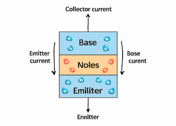
- Emitter: This region is heavily doped and supplies a large number of charge carriers (electrons) into the base.
- Base: This is the central, thin, and lightly doped region (usually P-type) that controls carrier flow. Its main job is to allow just enough recombination to regulate the current.
- Collector: This region is moderately doped and slightly larger than the emitter so it can collect the electrons and dissipate heat.
The physical construction of the device is such that a thin layer of P-type material is sandwiched between two thicker N-type layers. Each region is connected to a terminal: emitter, base, and collector, respectively.
NPN Transistor Symbol
The NPN transistor symbol comprises three terminals. The key feature is an arrow on the emitter leg, pointing outward (showing electron flow from emitter to outside). This distinguishes it from the PNP transistor.
How Does an NPN Transistor Work?
An NPN transistor combines two functions depending upon the way voltages are applied to the pins:
- The base-emitter junction is forward-biased (a small amount of voltage is applied, so the electrons can move in a manner that generates electrical current through the circuit).
- The collector-base junction is opposite-gridded (SRS a greater potential positive voltage on this collector attracts the electrons across the base to the collector).
Step-by-Step Working:
- Forward Bias at emitter-base: Emitter-Base—As soon as you put a small positive bias between the base and the emitter (VBE, typically 0.6-0.7V in silicon integrated circuits), electrons are pushed out of the emitter into the base.
- Thin and Lightly Doped Base: The base is extremely thin and lightly doped so very few electrons are recombining with holes in the base.
- Collector Attraction: The most electrons tumble in at the base towards the collector, which is at a higher voltage (reverse bias). This becomes the collector current (IC) that is much greater than the base (IB) current that is small.
- Indicator of Current Flow: The total current flowing on the collector and the base is called the emitter current (IE):
IE=IB+IC
IE=IB+IC.
This action means that a tiny current at the base can control a much larger current flowing from collector to emitter—this is the principle behind amplification.
NPN Transistor Operating Modes
Transistors, including NPN types, operate in three primary modes:
- Active Mode: Emitter-base forward biased, collector-base reverse biased. Used for amplification.
- Cutoff Mode: Both junctions are reverse biased. The transistor is OFF; no current flows.
- Saturation Mode: Both junctions are forward biased. The transistor is ON, allowing maximum current flow; it is used as a switch.
NPN Transistor: Key Features and Advantages
- High switching speed: Due to electron mobility, NPN transistors can switch much faster than their PNP counterparts.
- High current handling: NPN transistors handle higher collector currents efficiently.
- Cost-effective and easy to manufacture: Easier and cheaper to make, especially in silicon technology.
- Compatibility with integrated circuits: They are the preferred choice in most digital and analog ICs.
Applications of NPN Transistors
The generalized use of the NPN transistor in its many practical applications makes it a utilitarian transistor in every electronics field:
Amplifiers
Transistors, in the shape of NPN, are the main component of an amplifier circuit. They are capable of enhancing faint electronic signals and hence are applicable to radios, audio gadgets and communication devices. This is because they have high current gain and thus, are suitable for this job.
Switches
NPN transistors are fast switches in digital circuits. It is ideal in logic gates, microprocessor and power regulation because a small control signal at the base turns the device ON or off.
Oscillators
Signal generators and clocks, more often than not, use oscillator circuits with an NPN transistor being the active component to generate a stable signal at a particular frequency.
Current and Voltage Control
Voltage regulators used in power supplies and to produce precision current sources and mirrors are usually made by using NPN transistors, aiding in the prevention of voltage or current variations in sensitive circuits.
Digital Circuits
Other digital elements, such as logic gates and flip-flops, also involve NPN BJTs to a large extent. They are used on a constant basis due to quick switch time and convenience; thus, they are building blocks of computers and embedded devices.
Motor Drivers, Relay Drivers
Being able to interface motors or relays directly eliminates the need for microcontrollers and small signal devices to drive larger loads.
Sensors
NPN-transistor outputs are seen in some proximity and photoelectric sensors, particularly to provide a so-called current sinking behavior (a path to ground).
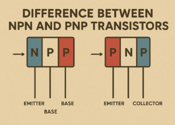
Differences Between NPN and PNP Transistors
Understanding how NPN and PNP differ helps in selecting the right device:
| Feature | NPN Transistor | PNP Transistor |
| Charge carriers | Electrons (majority) | Holes (majority) |
| Current flow | From collector to emitter | From emitter to collector |
| Symbol arrow | Outward (from emitter) | Inward (towards emitter) |
| Switching speed | Faster | Slower (generally) |
| Typical use | Most digital and analog circuits, standard semiconductor ICs | Complementary or where positive switching is required |
| Manufacturing cost | Lower | Higher |
| Preferred in ICs | Yes | Less preferred |
Reasons for Wide Use and Popularity
- Ease of manufacturing and high performance with silicon: Silicon is more suited for NPN construction due to higher electron mobility.
- Superior switching and amplification: NPN transistors can efficiently amplify weak signals and act as fast switches.
- Widespread availability: Most transistors in commercial ICs and discrete forms are NPN due to their advantages.
Practical Example: NPN Transistor as a Switch
Imagine you need to switch an LED with a microcontroller, which can only sink a low current. You can add the microcontroller output to the base of an NPN transistor (via a current-limiting resistor) to use the transistor to switch a much larger current in the LED, turning it ON and OFF with the tiny signal generated by the microcontroller.
Conclusion
The NPN transistor is the main pillar of modern electronics. This, along with its capacity to switch and amplify currents fast with high efficiencies, has ensured its widespread use in most applications, such as audio amplification, computer logic circuits and power control. Whether it is sophisticated microelectronics or simple circuits, knowing how the NPN transistor does its job puts you in the right position to exploit it to its furthest limits in a wide variety of electronic applications.
FAQs
Q1. What is an NPN transistor and how does it work?
An NPN transistor is a form of the bipolar junction transistor in which current between the collector and emitter may be directed when the base is positive with respect to the emitter.
Q2. What are the main parts of an NPN transistor?
An NPN transistor consists of three terminals; those include the emitter, base and collector. Electrons are released by the emitter, flow is limited by the base, and the current is collected by the collector.
Q3. Where are NPN transistors commonly used?
NPN transistors find extensive use in amplifiers, digital circuits and switch applications because they can switch large current with a small input signal.
Q4. How is an NPN transistor different from a PNP transistor?
Under NPN, positive base current flows from the collector to the emitter. In PNP, the current is fed from emitter to collector by negative base voltage.
Q5. How do you identify an NPN transistor symbol?
NPN transistor symbol also shows a direction that current goes outwards with an arrow out of the emitter; this is what distinguishes it from the PNP transistor symbol.
Also Read
Difference Between NPN and PNP Transistors
PNP Transistor
NPN Transistor
What is a Transistor
What is Fet?
Bipolar Junction Transistor (BJT)
Characteristics of a Transistor
Uses of Transistors